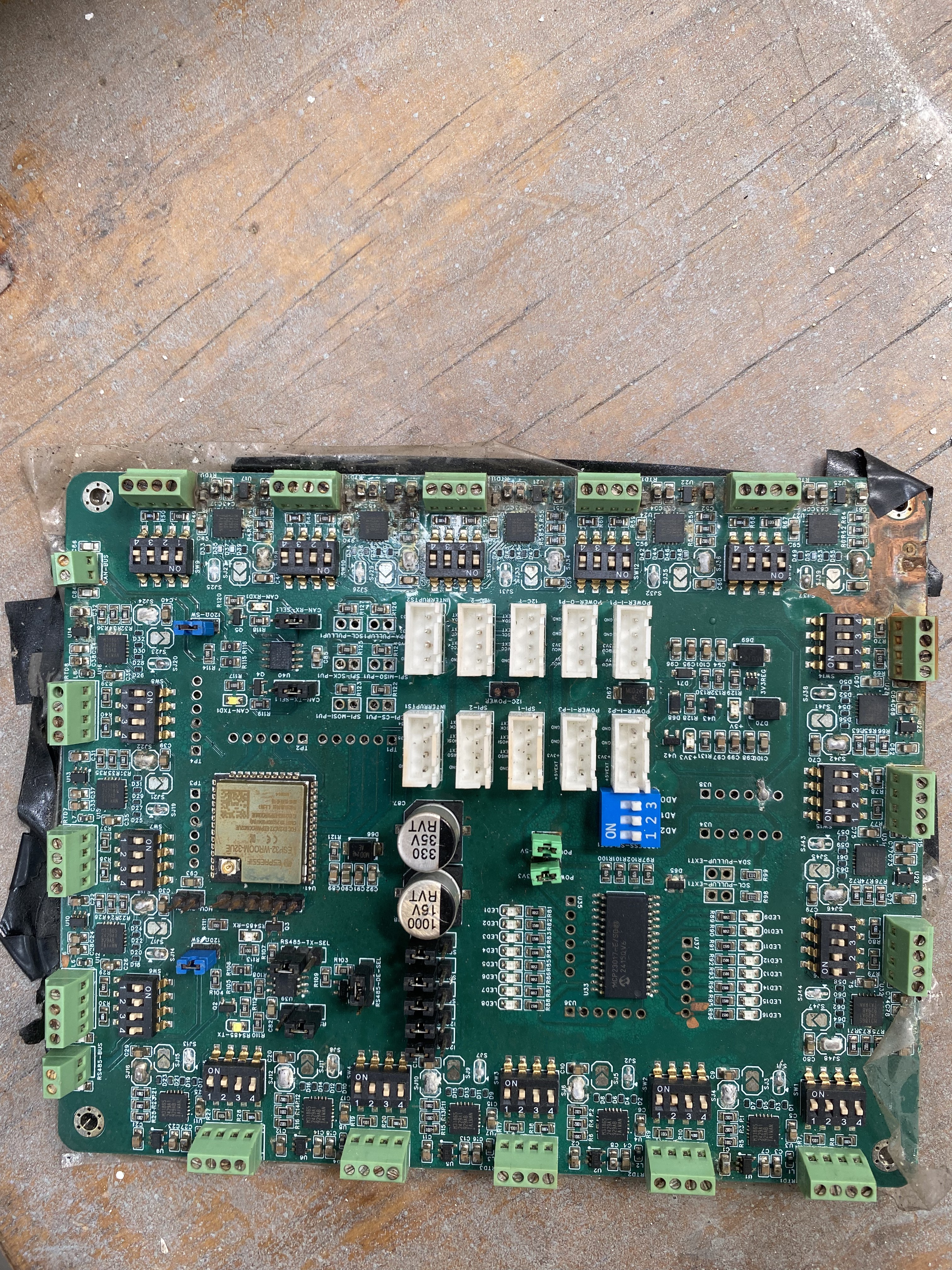
I built the 32-channel RTD module because I had a measurement problem.
At the direct air capture plant, we needed to map the thermal gradient across an adsorbent bed during regeneration — the cycle where you drive heat through the material to release captured CO₂. That means a lot of temperature sensors, read simultaneously, across a dense physical space. Off-the-shelf data acquisition systems either couldn't handle 32 channels without daisy-chaining multiple units, or were priced for lab environments where nobody cares about per-unit cost at scale.
So I designed the board from scratch. 32 channels of per-channel signal conditioning, a multiplexed ADC, and a dense terminal block layout that let you land 32 PT100 RTD cables in one place without it turning into a wiring disaster.
That part was straightforward. The interesting part came after.
Why the board sees what the plant sees
DAC plants run thermal cycles constantly. Adsorption at ambient. Regeneration at 100°C+. Cool down. Repeat.
That cycle is the whole product. Everything is designed around running it as fast as possible, as many times as possible, for as long as possible.
Which means any hardware inside the machine runs that cycle too.
A PCB sitting inside a process enclosure experiences every temperature swing the machine goes through. Expand, contract. Expand, contract. The FR4 substrate, the copper traces, the solder joints, the component packages — all of them have slightly different thermal coefficients. Every cycle accumulates a little mechanical stress. The question is where that stress goes, and how long before something gives.
This isn't a novel problem. IPC and MIL-SPEC standards have been dealing with it for decades. But most of that literature is for aerospace and defence hardware, where you have big qualification budgets and small unit volumes. We were building towards a fleet of machines. I needed to know what our actual failure modes looked like before we were discovering them in the field.
The test
We ran 450+ cycles. Ambient to somewhere north of 100°C, back to ambient. The board was powered throughout.
I wasn't running a pristine lab setup. This was inside a working plant enclosure, with real sensor loads on all 32 channels, real cable bundles landing on the terminals, and real vibration from the fans and heaters running around it. That felt more honest than a controlled thermal chamber would have been.
After 450 cycles, the board looked like it had been somewhere. The solder mask picked up the grime that accumulates in any industrial environment. A couple of the terminal blocks showed mechanical wear from repeated cable insertions and the small movements that come with thermal expansion.
But electrically, all 32 channels were still reading.
No trace failures. No cold solder joints that had crept open. No delamination bubbling up at the edges or around the vias. The multiplexed ADC was still converting cleanly. Calibration drift was within normal instrument tolerance — nothing I could attribute specifically to the thermocycling.
What held up
There are a few design decisions that I think contributed to this.
The terminal blocks were rated well above the operating voltage and current — not because the signal levels demanded it, but because I wanted the mechanical clamping force to hold up through repeated temperature swings. Cheap terminals loosen. Loose terminals mean intermittent contact, which in a temperature measurement context is exactly the failure mode that's hardest to catch because it mimics a sensor problem rather than a board problem.
The signal conditioning components were placed and routed to keep thermal gradients across the board as uniform as possible. Uneven heating creates differential expansion, and differential expansion is where trace stress concentrates. I wasn't doing finite element analysis on the thermal distribution — this was more intuition from having debugged enough PCB failures — but the layout ended up with the heat-generating components reasonably distributed rather than clustered.
And I used conservative design rules throughout. Wider traces than strictly necessary. Generous via diameters. Thermal reliefs on the pad connections to the plane layers. None of this is heroic engineering. It's just not trying to be clever when reliability is the constraint.
What I'd change
What I'd change for the next version: the board thickness. We used standard 1.6mm FR4. Under thermocyclic load, thicker boards resist warping better, and warping is one of the failure modes you start to see on large-footprint boards with high copper pour coverage. At 450 cycles we weren't seeing it, but if this goes to 2000+ cycles over a machine lifetime, I'd want to qualify it properly and probably move to 2.0mm.
The other thing I'd do is add a dedicated thermistor on the board itself to log the actual temperature the PCB is experiencing during operation. Right now I'm inferring it from the enclosure temperature. A direct measurement would let me correlate any future failures to actual thermal exposure rather than nominal cycle parameters.
Still in service
450 cycles is not a long test. A machine running two regeneration cycles per day would hit that in less than a year. We need this hardware running for years.
But it was enough to tell me the design was in the right direction — that the failure modes we'd worry about at 450 cycles weren't happening, which meant we could focus on the failure modes that might show up later rather than fixing obvious problems early.
The board is still in service.